

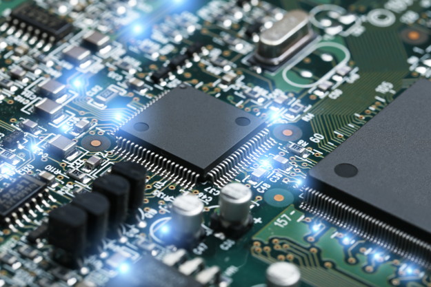
Chinese calligraphy is appreciated as a supreme form of art which takes a precisely ordered arrangement of strokes and dexterity, with the help of ink and a brush, to complete an exquisite work. Industrial processes such as photolithography are delicate and intricate enough to be regarded as a kind of workmanship which requires also complex coordination of equipment and skills. The craft work of electronics fabrication is beyond simple. Who would have given a thought to using normal black ink to optimise the process while doing calligraphy writing? However, researchers from The Chinese University of Hong Kong (CUHK) have found that ink is an effective and optimal agent readily available for producing compact chips, restoring connections of cracked electrical lines on circuit boards and even in accurate medicine devices, amidst complicated scientific procedures.

Penmanship in Physics
The conventional deposition process used in current fabrication technology has always been a hurdle to leap if one is to manufacture miniature chips. From photoresist, to evaporation, to lifting off, these chemical procedures give rise to uncertainty over or even failure in perfect quality, not to mention meeting expectations in crafting a pattern of microscopic size on a circuit board. It is in fact harder than writing on a hair strand which carries a diameter of 0.18 millimeters.
The core leader of the research team, Professor Yang Sen, Assistant Professor of CUHK Physics who is a handcraft enthusiast pointed out another great challenge, “(In quantum optics,) we also talk about accurate positioning. Current protocol cannot afford precise positioning with high resolution due to the complexity and harsh criteria.” The normal calligraphy ink brings the team a new hope.
Professor Xia Kangwei from the University of Stuttgart, is also a former Research Assistant Professor of the Department of Physics at CUHK. He is a member of the team and hit upon this idea of how far ink could go in the field of photolithography while he was once practicing Chinese calligraphy at home. It was a totally unexpected brainwave for the research team.

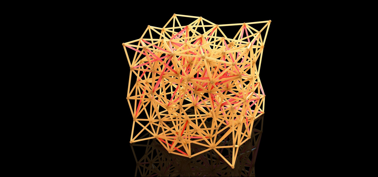
After multiple rounds of research and tests on mechanics, electromagnetics and heat, to the team’s surprise, random calligraphy carbon ink bought, from a stationery store, carried the core quality that they needed – semiconductor nanoparticles. “The nanoparticles have a minimal size of less than 100 nanometre (nm) with very high precision, which was a shock to us.” said Professor Yang. He added, “With this, we can even draw lines and dots of a size less than 1 nm. Complex drawings and diagrams are not a challenge to us”. Chen Yifan also a member of the research team, who gave the demonstration said, “The CUHK emblem written in platinum is of a total size of 250 micron (um), equivalent to 12 strands of human hair. To look into details of it, you will need a microscope.”

With the application of a simple laser writer/printer, carbon ink acts as very good adhesive agent to blend with different metallate to form the “universal ink”. In a nutshell, the photo-electrical effect helps change the metal ion in the “universal ink” into metal itself and the laser light can push those particles to your desired position on substrates like glass, quartz, and tape. In this case, you do not have to limit yourself in the choice of metal usage or worry about the incompatibility of metals with different material compositions.
The potentiality of this new mechanism also carries another two exceptional advantages – low production cost plus green value for the environment. The only specified conditions for deploying this technology are a home-built laser writer and calligraphy ink, commercially available everywhere. Not even an expensive clean room is needed. Further, unlike the traditional photolithography process which produces solvent and chemical wastes that harm the environment, the residue solution left after deposition under the deposition method can be washed away and recycled without much waste and pollution.
This simplified and greater ease of manufacture that spares money, labour and time actually gives a push to the industry. It is applicable to many features from prototyping to customised wearables like clinical hearing aids, or even to jewelry. Some may worry that the chip-making technology has hit a ceiling. It should not be of high concern from now on.


Pioneering a New normal in Industry with a Snoopy State of Mind
Having obtained his doctorate degree in the USA and postdoctoral research fellowship in Germany, Professor Yang came to CUHK in 2016. He believes that curiosity is his major motivation in furthering his passion in physics. “It is a plaything, and our group carries an inquisitive mind on everything and we all do this for fun!” asserted Professor Yang. And this is how the research team came to link the seemingly irrelevant calligraphy ink with industrial advancement. This novel project has been published in Nature Communications and the University has filed a patent for this new technology. A full version of the study can be found here.